
Read the silicon carbide epitaxial in one article - the high value of the silicon carbide power semiconductor industry chain!
SiC power semiconductors are a “golden track” with high growth potential. In 2024, the global silicon carbide power semiconductor market was only 2.55 billion US dollars. In 2029, the global silicon carbide power semiconductor market will exceed 13.5 billion US dollars. In just 6 years, in 2035, the market size will soar to 115 billion US dollars, and the growth momentum is particularly rapid.
However, many people have misunderstood the value core of the silicon carbide industry chain — in this huge industrial chain, it is the silicon carbide epitaxial link that actually determines the upper limit of device performance, opens up the enterprise gap, and controls the core value. As the core functional area of silicon carbide power devices, customized silicon carbide epitaxial is a “safety dam” for the stable operation of high-voltage power equipment, which determines the value of silicon carbide power semiconductors.
Currently, the value of the 1200V epitaxial layer for vehicles is greater than that of the substrate, and the 3,300V epitaxial layer for solid state transformers is already more than three times that of the substrate! As voltage levels increase, epitaxial's share of total chip costs will continue to rise sharply. Outreach is a veritable “highland of value” in the entire industrial chain.
There is no doubt that whoever has the leading edge in silicon carbide epitaxial will have a voice in the future of the global silicon carbide power semiconductor industry! Today, we are abandoning obscure technical terms and using popular vernacular and intuitive lifestyle analogies to take everyone to deeply understand the core value, industrial logic, and investment potential of silicon carbide epitaxial.
Silicon carbide epitaxial is a high-rise building on the “foundation” of the substrate. Thickness and structural complexity determine the upper value limit
To understand silicon carbide epitaxial, we must first disassemble and understand the basic logic of the silicon carbide industry chain.
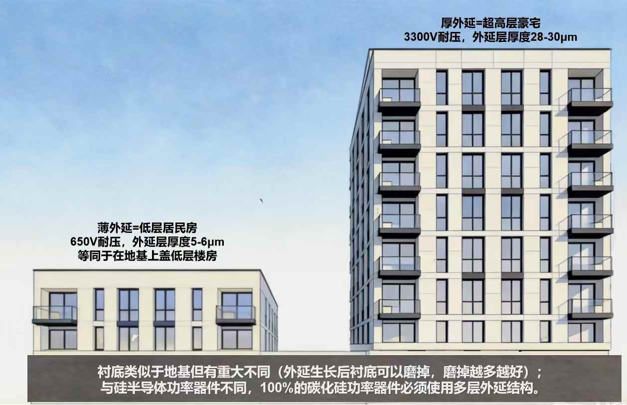
If a silicon carbide power device, the core for efficient conversion and control of electric energy, is compared to a complete building, the silicon carbide substrate can be compared to the foundation of a building, and the silicon carbide epitaxial layer can be compared to a single-layer or multi-layer structure of a building.
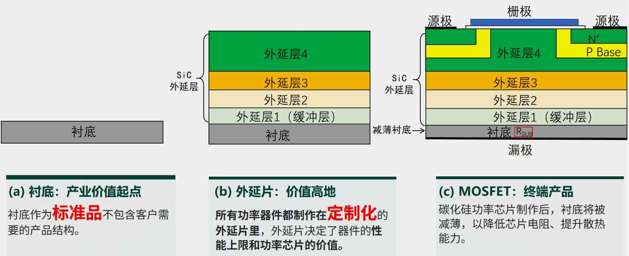
As a single crystal substrate, the silicon carbide substrate is a standard product. The substrate does not include the product structure required by the customer. What really determines device performance and creates core value is the next epitaxial step.
The so-called silicon carbide epitaxial, in simple terms, is a customized multi-layer silicon carbide single crystal structure with higher quality and more controllable electrical parameters according to the customer's specific needs through a precise chemical vapor deposition process. The substrate wafer is combined with the epitaxial structure, which is an epitaxial film. The silicon carbide quality of the epitaxial layer must be significantly higher than that of the substrate, and a large number of defects in the substrate must be eliminated or some defects in the substrate must be locked up and not entered into the epitaxial layer. Without exception, all silicon carbide power devices are made in an epitaxial layer. After the device is manufactured, in most cases, the substrate is thinned and worn out, so that the resistance and thermal resistance caused by the substrate can be eliminated as much as possible. For the ultimate silicon carbide power device, its core performance, such as voltage resistance, switching efficiency, and energy loss, are all determined by the epitaxial layer, and its quality directly determines the maximum performance that the device can eventually achieve.
An analogy with a building: if a low-rise residential house is built on a foundation, the building value of the foundation and the ground are about the same, accounting for 50% each. Similar to the current value ratio of silicon carbide substrates and thin epitaxial layers in low-voltage devices, each accounting for 50%. However, if a super mansion over 30 stories high is built on the same foundation, the value of the building on the ground will inevitably be much higher than the value of the foundation. The substrate is the “foundation” with a fixed input, and the epitaxial layer is the “floor” above the foundation. The structural complexity and total thickness of the epitaxial layer is the structure and total height of each floor. How thick and how good the quality of the epitaxial layer can be determines how much value you can create on this “foundation.”
Back to the data of silicon carbide power devices: According to statistics, 1200V automotive devices require a 10-13 μm thick epitaxial layer; 1500V photovoltaic inverter devices require a 13-15 μm epitaxial layer; while 3300V high-end devices for industrial and power grids require a 30-32 μm thick epitaxial layer, and ultra-high voltage devices of 10,000 volts or more require a total epitaxial thickness of about 100 μm. Currently, the value of the 1200V epitaxial layer for vehicles is greater than that of the substrate, and the 3,300V epitaxial layer for solid state transformers is already more than three times that of the substrate! As the voltage level increases, epitaxial's share in the total cost of the chip will rise dramatically, making it a veritable 'high value'.
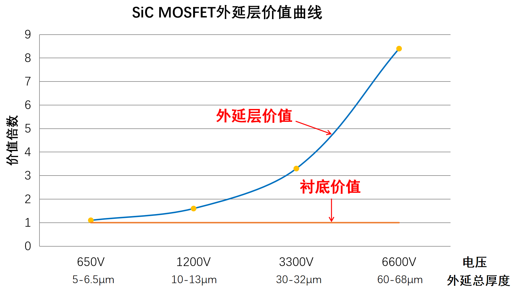
On a substrate of the same specification, the greater the total thickness of the epitaxial layer growth, the more complex the structure, and the greater the corresponding commercial value and industrial value.
Under the trend of high pressure industry, thick epitaxial layers are the core of cost reduction and efficiency
After reading the previous article, you may have two questions: Why is the thicker the epitaxial layer, the higher the voltage it can withstand? The higher the voltage the epitaxial layer can withstand, and what is the better? Next, we will use our middle school physics knowledge, combined with practical applications in the industry, to clearly explain this matter.
1. Why is the thicker the epitaxial layer, the higher the pressure rating?
The core work of silicon carbide power devices is to act as a “switch” and “isolation” in high-voltage circuits, and to ensure that the device can work properly at a high voltage of several kilovolts or even tens of thousands of volts without being broken down, a special “pressure-resistant layer”, that is, a silicon carbide epitaxial layer.
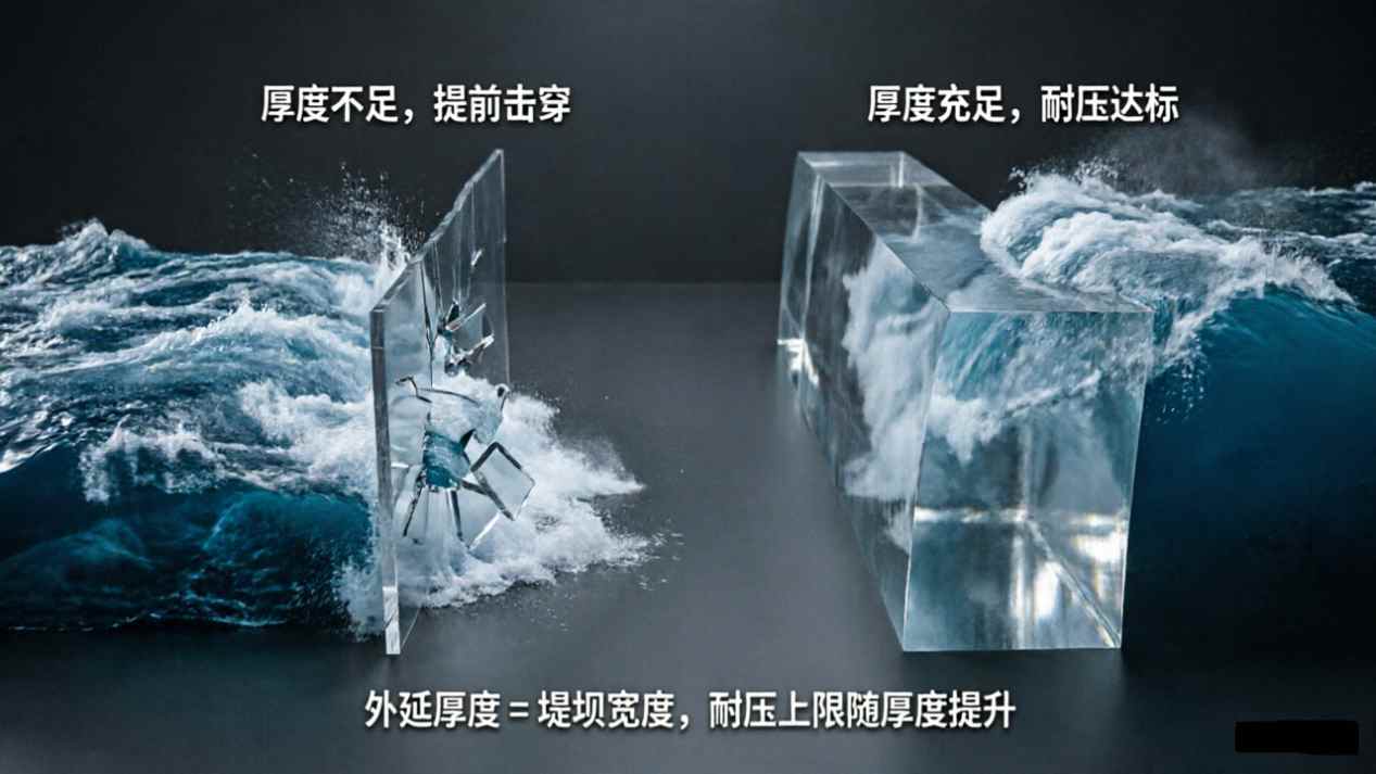
If you compare high-voltage electricity to a raging flood, the epitaxial layer is a dam that blocks the flood. The thicker and stronger the dam, the higher the flood level that can be blocked, and the less likely it is for the dam to collapse; similarly, the thicker the silicon carbide epitaxial layer, the higher the upper limit of voltage it can withstand, and the more stable and safer the device is under high pressure operating conditions. Here is a very critical difference from building a house on a foundation. As mentioned earlier, the substrate will be thinned or worn out after the device is made, and the performance of the device will be better after the substrate is thinned or worn out.
Of course, the technical research problem of thick epitaxial is far more than “long and thick” — it is necessary not only to meet the thickness standards, but also to ensure low defects and high uniformity of the crystals at large thicknesses. Otherwise, it will be like a “tofu scum dyke”. Even if it is thick enough, it will be broken through the defects. This is why high-end thick epitaxial technology has always been one of the core barriers in the silicon carbide industry chain.
The core of epitaxial competition is the need to try our best to improve yield so that all epitaxial films produced are qualified “dams”. This is extremely difficult in terms of engineering. Since epitaxial growth requires extremely high defect control, 'yield' directly determines the profit level of an enterprise. The industry generally has the phenomenon of “easy access to equipment and hard to find yield”, which has also built a moat for leading companies.
The extremely high technical threshold makes epitaxial foundry the most concentrated link in the silicon carbide industry chain. According to Insight Consulting data, the top five global silicon carbide epitaxial foundry companies will collectively occupy 93.4% of the market share in 2024 — which means that “yield is a moat” is the most extreme in the epitaxial process. Among them, the three companies with the highest global market share are China's Hantian Tiancheng (02726) accounting for 31.6%, Japan's Resonac (4004.T) accounting for 19.4%, and China's Hebei Puxing accounting for 17.8%.
2. Why is the higher the voltage, the better? Understand what the industry needs from physical principles
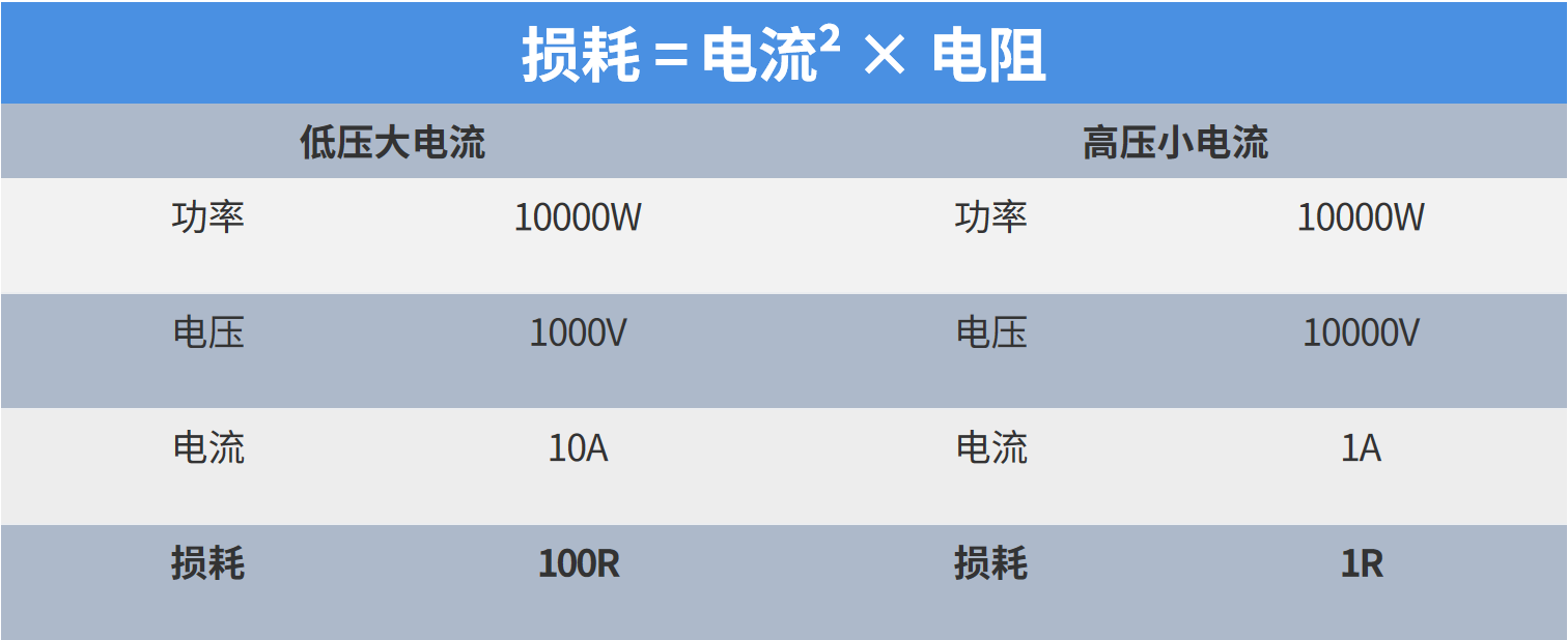
Using only Ohm's law and the basic principles of energy loss we learned in middle school, we can understand the essence of pursuing high voltage at a glance: P = V x I, P represents power (watts), V represents voltage, and I represents current. For the same power, as the voltage V increases, the required current I can be reduced. Furthermore, middle school physics tells us that the loss of energy is equal to the square of the current times the resistance: I²×R, that is, the loss of energy is directly proportional to the square of the current.
Look, based on middle school physics, we can draw an obvious conclusion: for power systems with the same power, the higher the voltage used, the less current required; the smaller the current, the lower the energy loss.
For example, for a 10,000 watt power system, when we use a voltage of 1000V, the current in the system circuit is 10A, and the loss at this time is 10²×R=100R; and when we raise the voltage to 10000V, the current drops to 1A. The loss at this point directly becomes 1²×R=1R, and the loss is directly reduced to 1% of the original!
This is the core value of high pressure: it can greatly reduce energy loss, greatly improve energy efficiency, and at the same time reduce the heating of lines and devices, extend the service life of equipment, reduce equipment volume, and most importantly, reduce production costs. Therefore, a large number of applications in the silicon carbide industry have been developing towards high voltages. For example, new energy vehicles were upgraded from the original 400V platform to the 800V high voltage platform, and further upgraded to the 1000V voltage platform. Grid-connected silicon carbide devices for photovoltaic wind power have been upgraded from 400V to 1700V, or even 2000V. The core reason for AI data centers and power grids to promote high voltage solid state transformers (SST) is also based on the need — efficiency, energy saving, and cost savings. Following the high voltage route is an inevitable development direction for a large number of power applications.
According to CICC's research findings, silicon carbide power chips are the core components of AI power supply systems and will be widely used in the computing power center construction boom. Starting in 2026, the demand for silicon carbide power chips in AI data centers will increase rapidly, and the compound growth rate for silicon carbide chips per megawatt of computing power is expected to exceed 80% from 2026 to 2030; at the same time, due to the continuous increase in chip voltage resistance requirements, the average value of a single silicon carbide chip used in AI computing power centers will also increase at the same time, driving the overall compound value of silicon carbide chips corresponding to each megawatt to 140% to 380%. As volume and price rise sharply, the value share of silicon carbide power semiconductors in the AIDC industry chain will continue to increase. Looking further, the epitaxial link is the core of determining the voltage resistance level of silicon carbide power chips, so it will also be the upstream link that benefits most significantly in the development of the AIDC industry.
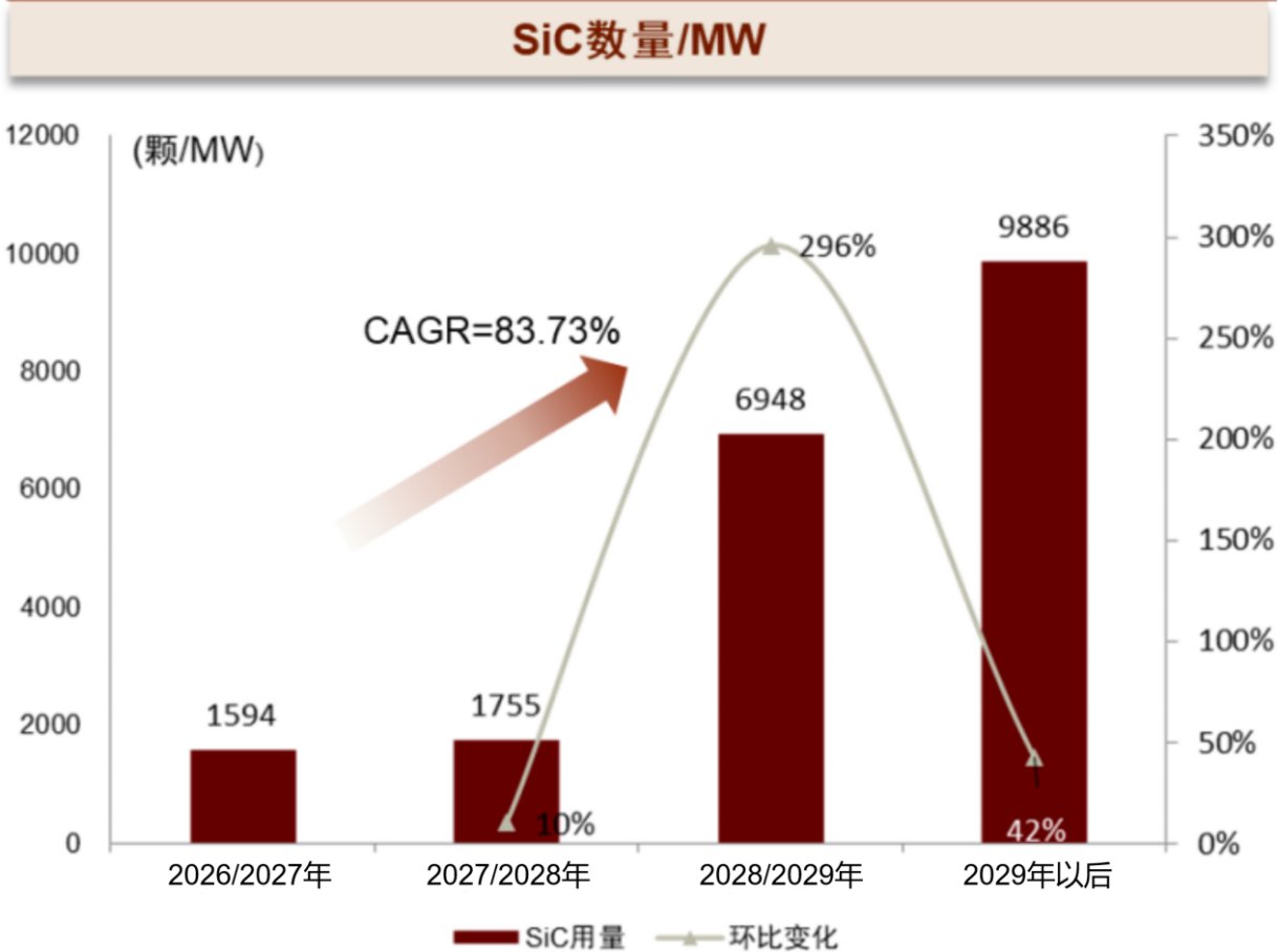
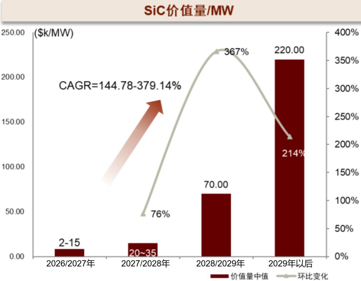
Photo Caption: Silicon carbide usage and value in response to changes in AIDC's power supply architecture (Source: CICC Research Department)
All in all, if silicon carbide substrates are a “standardized foundation,” then silicon carbide epitaxial is a “high-value building” built on a “standardized foundation”. It is not only a core gripper for industrial upgrading, but also a core value high for future silicon carbide power semiconductor tracks. The long-term growth certainty and industrial strategic value are outstanding.