
Investment of 550 billion US dollars from power plants to chips: US and Japan are rumored to be negotiating to build a new semiconductor factory, GFS.US (GFS.US) plans to operate it
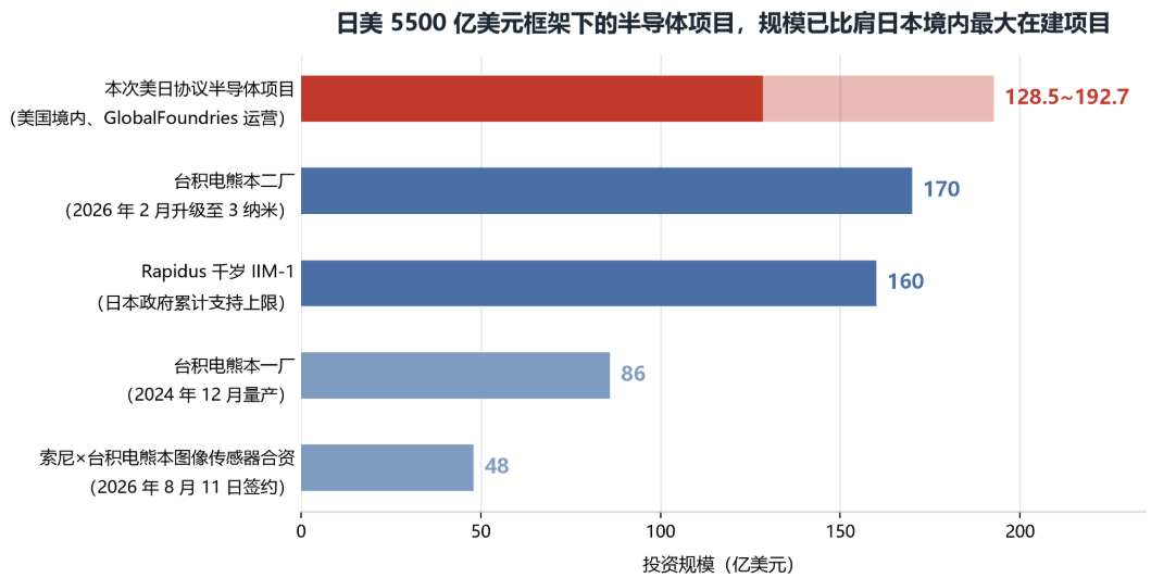
The Zhitong Finance App learned that, according to sources, Japan and the United States are currently discussing the construction of a semiconductor factory. The project is part of a $550 billion investment agreement between the two countries. The project is estimated to be worth 2 trillion to 3 trillion yen (about 12.85 billion to 19.27 billion US dollars), and will be operated by chip manufacturer GFS.US (GFS.US), focusing on logic chips. If it finally comes to fruition, this will be the first semiconductor project under the $550 billion framework — it is also the first step in shifting from a power plant to a chip factory in this investment plate underpinned by “buying American goods.”
How to spend $550 billion
First, explain the framework clearly. In July 2025, in tariff negotiations with the US, Japan promised to invest 550 billion US dollars (about 86 trillion yen, equivalent to about 12% of Japan's GDP) in exchange for the US to reduce basic tariffs on Japan to 15%.
On September 4, local time, Trump signed an executive order to officially implement the US-Japan trade agreement. The attached memorandum of understanding describes the investment mechanism quite specifically: Japan must disburse funds before the end of Trump's term (January 19, 2029); the US president has the final authority to decide on project investment, an investment committee under the Department of Commerce is responsible for recommending and supervising each project, and establishes a special purpose company for each project; the profit of the project is divided equally between Japan and the US until Japan recoups the principal and interest of the investment. 90% of the profits go to the US and 10% to Japan; Japan has the right to refuse to fund a certain project However, the US can impose tariffs on Japanese products as a countermeasure.
The actual implementation is more “energy” than the framework: almost all of the 6 projects in the first and second batches that have been announced previously focused on power generation and energy infrastructure.
The largest single is in Ohio — the 9.2 gigawatt gas power plant, at a cost of 33 billion US dollars, was developed by SoftBank's SB Energy. OpenAI has signed a 20-year lease and Nvidia promised to take over under specific circumstances. If built, it will be the largest gas-fired power plant in US history, generating enough power to cover the two cities of New York and Los Angeles; the 5.2 GW and Pennsylvania project was built by NexTERA and has received the first $3.33 billion — of which 6.3 billion US dollars has been received One hundred million dollars comes from loans from the Japan Bank for International Cooperation (JBIC), and another 1.26 billion US dollars is provided by private syndicates composed of Citibank, J.P. Morgan Chase, etc., and underwritten by Japan Export and Investment Insurance (NEXI). The first batch of electricity targets to be connected to the grid in 2028.
Turning to semiconductors: Akazawa Ryomasa “AI and semiconductors will account for a very large share in the future”
The direction of the wind has changed. Japan's Minister of Economy, Trade and Industry Akazawa Ryomasa met separately with US Secretary of Commerce Lutnick and Trade Representative Greer in Washington from September 3 to 4. The two sides confirmed the progress of the six projects already disclosed and said they are selecting a new batch of investment projects. According to reports, Akazawa said at a press conference on September 4, “AI and semiconductor manufacturing will account for a very large share in the future.” He also added that “it will take some time to improve the project” — the specific list of the third batch of projects was not announced with this report. At the same time, both sides confirmed that even if the US imposes new tariffs in the future, the tariff level on Japan will still strictly abide by the 2025 agreement and not exceed the 15% upper limit.
The report also mentioned that the list of projects discussed by the two countries under this framework also includes a large-scale data center construction project involving the SoftBank Group.
Why GF: Not a 2nm core US foundry
The operator's choice of GF is intriguing. This foundry, headquartered in Malta, New York, withdrew from the advanced process competition in 2018. Instead of competing with TSMC and Samsung, it specializes in specialty processes and advanced packaging such as injection frequency, power management, and silicon photonics — the factories are distributed in the US (New York, Vermont), Dresden, and Singapore, Germany. It is one of the few pure foundry plants headquartered in the US and has substantial production capacity in the US.
In recent months, it has come very close to the US government: it received $1.5 billion in “Chip Act” production capacity subsidies in 2024; signed a $300 million letter of intent with the US Department of Commerce on July 29 this year to promote advanced packaging such as silicon photons, optical materials, and 3D hybrid bonding to serve near-package optics (NPO) and co-package optics (CPO) for AI data centers; it also finalized a $375 million quantum computing R&D agreement on September 8 — two additional government support totaling $675 million Disbursed by the Film R&D Office.
Fundamentally, GF is one of the few “non-advanced process” beneficiaries in the AI narrative: second-quarter revenue of $1.79 billion, up 6% year over year, and adjusted earnings of $0.46 per share, exceeding market expectations of $0.43; communications infrastructure and data center revenue surged 62% year over year, and the company raised the sector's annual growth rate guide to 50%-60%; silicon photon and germanium silicon production capacity has all been sold out until 2027. The drag is also obvious: due to the increase in storage prices, the smartphone business's revenue for the full year 2026 is expected to decline by a low double digit, and the automobile business fell 13% month-on-month in the second quarter.
Market Reactions and Institutional Views
There is a clear temperature gap between the capital market's pricing of GF and its narrative. As of the close of trading on September 16, GF reported $43.03 (up 0.65% on the same day), with a market capitalization of about $24 billion. It remained flat during the year, and the stock price was near the lower end of the 52-week range ($31.91 to $92.55). Before the Thursday market, GF shares rose 2.11% to $43.94 as of press release.
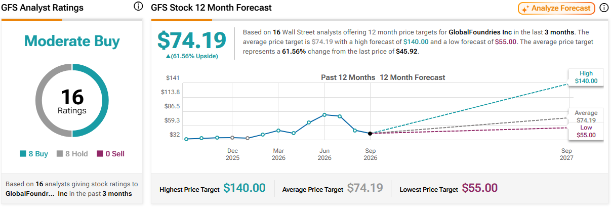
However, the seller's consensus was clearly more optimistic: according to investing data, 14 of the 22 covered analysts gave a purchase, with an average target price of $76, implying about 70% of the upside compared to the current price. According to Tipranks data, 8 of the 16 coverage analysts gave a buy and 8 gave a hold, with an average target price of $74.19.
Cantor Fitzgerald analyst C.J. Muse on September 8 reiterated the “increase” and target price of $90 on the grounds that “OEM production capacity continues to be tightened and there is no end in sight” — TSMC is raising prices by a high single-digit percentage, and the current supply gap is about 15%-20%, while Grofond's silicon photon/germanium silicon production capacity can support a business scale of about 4 billion US dollars (currently only 400 million to 450 million US dollars), and the ASP will increase from January 1.
Stifel first covered purchases on September 2, with a target price of $60; relatively cautious Morgan Stanley remains neutral, with a target price of $60; UBS, J.P. Morgan Chase, and Citibank are all neutral.
Risk Alerts
First, the news has not been officially confirmed — the factory site, technology node, and Japan-US investment ratio have not been disclosed, and it is still unknown whether the project will enter the third batch of official lists.
Second, “logic semiconductors” are not equal to advanced manufacturing processes: Grofond does not use 2 nm, and advanced logic production capacity in Japan is still betting on Rapidus (Chitose, Hokkaido, 2 nm, target mass production in the second half of fiscal year 2027) and TSMC Kumamoto Plant 2 (upgraded to 3 nm, total investment raised to about 17 billion US dollars, mass production in 2028) — this project is closer to the combination of “characteristic process logic+production capacity in the US”.
Third, Japan is not without opinion on this framework: Nobuhide Kiuchi, an economist at the Nomura Research Institute, wrote an article last year stating that the financing structure was “heavily biased against the US side”; Dennis Wamsted, an analyst at the Institute for Energy Economics and Financial Analysis (IEEFA), further bluntly stated that these power plants “will not be built on the scale of headlines,” and “this is essentially spending other people's money.” The US midterm elections are approaching, and the variables in the administration and tariff policy are the biggest discount of this 550 billion US dollars.